
-
mg电子老虎机彩票
-
通用型 SPST-NO(1a\2a)
-
通用型 SPST-NC(1b\2b)
-
通用型 SPST-NO+NC(1a1b)
-
-汽车应用
-
-增强隔离 3.75kVrms
-
-高灵敏度(低电流消耗)
-
-超低温/超高温工作(Topr - 40~110 ℃)
-
常用型光耦晶闸管输出光耦可控硅光耦晶体管光耦光伏光耦隔离放大器光耦IGBT驱动光耦MOSFET光耦IPMmg电子老虎机官方入口高速通信光耦光纤耦合器
Product line up
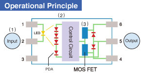
A PhotoRelays is a semiconductor relay with an LED as an input and MOSFET as an output.
|
|
Compared with Electro-Mechanical Relays
have moving contact: |
Compared with SSR (Solid State Relays) have phototriac for output: |
|---|---|
|
●Longer lifetime (No limit on mechanical and electrical lifetime) ●Higher-speed and high-frequency switching ●Higher sensitivity (less power consumption) ●Smaller size ●Less contact problems such as arcs, bounce, and noise ●More resistant to vibration and impact ●No limitation for the mounting direction |
●Able to control miniature analog signal ●Applicable to both AC/DC ●More sensibility ●Less leakage current ●Lower offset voltage ●Various contact structures such as 2a, 4a, 1b, 2b, and 1a1b in addition to 1a |
1.Technical Terminology
2.Reliability tests
mg冰球突破最新网址
mg电子老虎机老虎机
|
Term
|
Symbol
|
Description
|
|
|
Input
|
LED forward current
|
I
F
|
Current that flows between the input terminals when the input diode is forward biased.
|
|
|
LED reverse voltage
|
V
R
|
Reverse breakdown voltage between the input terminals.
|
|
|
Peak forward current
|
I
FP
|
Maximum instantaneous value of the forward current.
|
|
|
LED operate current
|
I
Fon
|
Current when the output switches on (by increasing the LED current) with a designated supply voltage and load connected between the output terminals.
|
|
|
LED turn off current
|
I
Foff
|
Current when the output switches off (by decreasing the LED current) after operating the device with a designated supply voltage and load connected between the output terminals.
|
|
|
LED dropout voltage
|
V
F
|
Dropout voltage between the input terminals due to forward current.
|
|
|
Power dissipation
|
P
in
|
Allowable power dissipation between the input terminals.
|
|
Output
|
Load voltage
|
V
L
|
Supply voltage range at the output used to normally operate the PhotoRelays.
Represents the peak value for AC voltages.
|
|
|
Continuous load current
|
I
L
|
Maximum current value that flows continuously between the output terminals of the PhotoRelays under designated ambient temperature conditions. Represents the peak value for AC current.
|
|
|
On resistance
|
R
on
|
Obtained using the equation below from dropout voltage V
DS
(on) between the output terminals (when a designated LED current is made to flow through the input terminals and the designated load current through the output terminals.) R on = V DS (on)/I L |
|
|
Off state leakage current
|
I
Leak
|
Current flowing to the output when a designated supply voltage is applied between the output terminals with no LED current flow.
|
|
|
Power dissipation
|
P
out
|
Allowable power dissipation between the output terminals.
|
|
|
Open-circuit output voltage
|
V
oc
|
Voltage required for driving a MOSFET
|
|
|
Short-circuit current
|
I
sc
|
Current that is output from the driver when the input is turned on
|
|
Electrical
characteristics
|
Turn on time
|
T
on
|
Delay time until the output switches on after a designated LED current is made to flow through the input terminals.
|
|
|
Turn off time
|
T
off
|
Delay time until the output switches off after the designated LED current flowing through the input terminals is cut off.
|
|
|
I/O capacitance
|
C
iso
|
Capacitance between the input and output terminals.
|
|
|
Output capacitance
|
C
out
|
Capacitance between output terminals when LED current does not flow.
|
|
|
I/O isolation resistance
|
R
iso
|
Resistance between terminals (input and output) when a specified voltage is applied between the input and output terminals.
|
|
|
Total power dissipation
|
P
T
|
Allowable power dissipation in the entire circuit between the input and output terminals.
|
|
|
I/O isolation voltage
|
V
iso
|
Critical value before dielectric breakdown occurs, when a high voltage is applied for 1 minute between the same terminals where the I/O isolation resistance is measured.
|
|
Ambient
temperature
|
Operating
|
T
opr
|
Ambient temperature range in which the PhotoRelays can operate normally with a designated load current conditions.
|
|
|
Storage
|
T
stg
|
Ambient temperature range in which the PhotoRelays can be stored without applying voltage.
|
|
Max. operating frequency
|
—
|
|
Max. operating frequency at which a PhotoRelays can operate normally when applying the specified pulse input to the input terminal |
mg冰球突破注册网站
|
Classification
|
Item
|
Condition
|
Purpose
|
|
Life tests
|
High temperature storage test
|
T
stg
(Max.) |
Determines resistance to long term storage at high temperature.
|
|
|
Low temperature storage test
|
T
stg
(Min.) |
Determines resistance to long term storage at low temperature.
|
|
|
High temperature and high humidity storage test
|
85°C
185°F , 85%R.H. |
Determines resistance to long term storage at high temperature and high humidity.
|
|
|
Continuous operation life test
|
V
L
= Max., I L = Max., I F = Recommended LED forward current |
Determines resistance to electrical stress (voltage and current).
|
|
Thermal
environment
tests
|
Temperature cycling test
|
Low storage temperature (T
stg
Min.) High storage temperature (T stg Max.) |
Determines resistance to exposure to both low temperatures and high temperatures.
|
|
|
Thermal shock test
|
Low temperature (0°C)
(32°F) , High temperature (100°C) (212°F) |
Determines resistance to exposure to sudden changes in temperature.
|
|
|
Solder burning resistance
|
260±5°C
500±41°F , 10 s |
Determines resistance to thermal stress occurring while soldering.
|
|
Mechanical
environment
tests
|
Vibration test
|
196 m/s
2
{20 G}, 100 to 2,000 Hz*1 |
Determines the resistance to vibration sustained during shipment or operation.
|
|
|
Shock test
|
9,800 m/s
2
{1,000 G} 0.5 ms*2; 4,900 m/s 2 {500 G} 1 ms |
Determines the mechanical and structural resistance to shock.
|
|
|
Terminal strength test
|
Determined from terminal shape and cross section
|
Determines the resistance to external force on the terminals of the PhotoRelays mounted on the PC board while wiring or operating.
|
|
|
Solderability
|
245°C
473°F 3 s (with soldering flux) |
Evaluates the solderability of the terminals.
|
*1 10 to 55 Hz at double amplitude of 3 mm for Power PhotoRelays. *2 4,900 m/s 2 , 1 ms for Power PhotoRelays.
